SK Hynix is making a substantial $13 billion investment effort to expand its footprint in the artificial intelligence (AI) memory supply chain, focusing particularly on the burgeoning market for high-bandwidth memory (HBM).
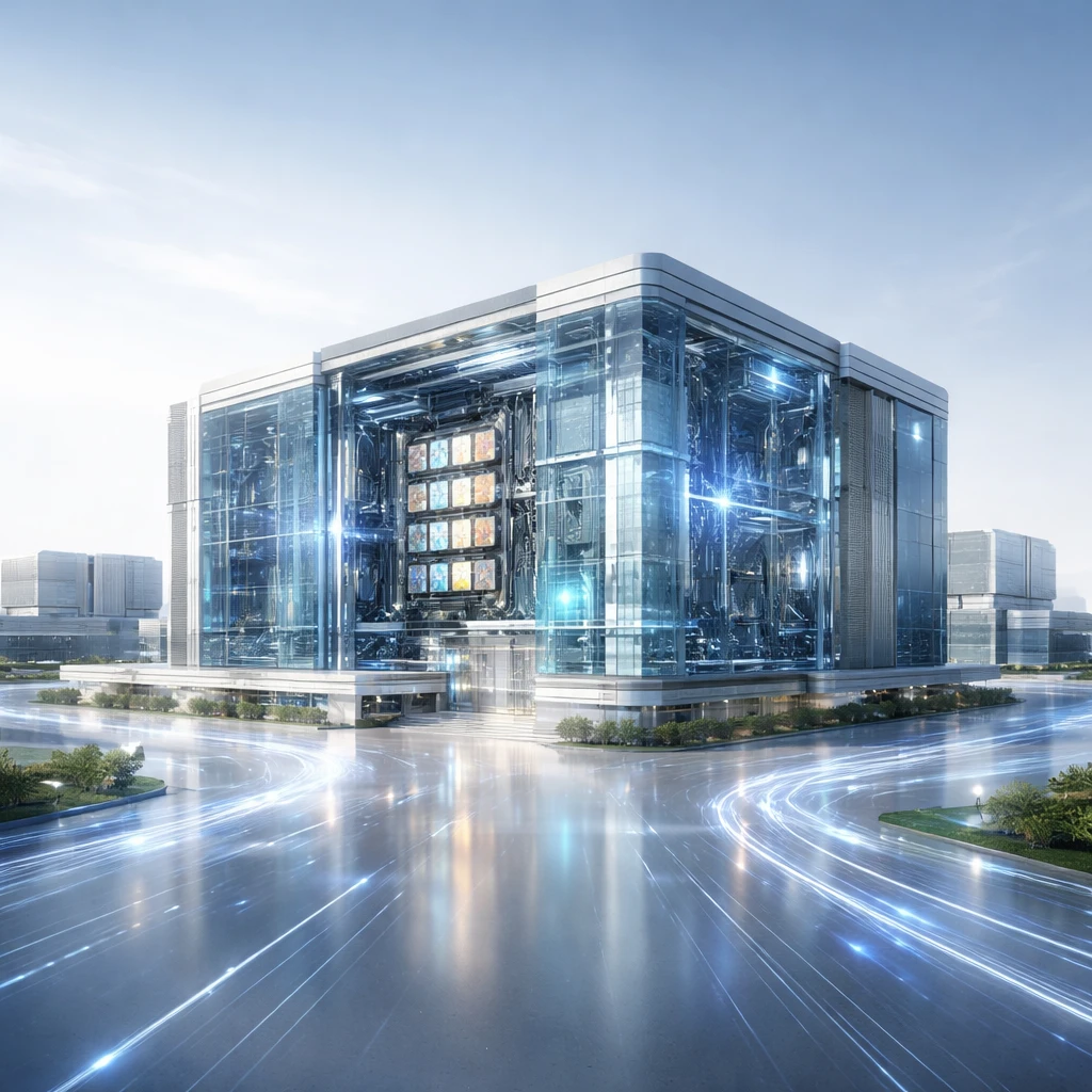
As one of the leading producers of HBM, SK Hynix has announced plans to build a new facility called P&T7, dedicated to advanced semiconductor packaging and testing. Located within the Cheongju Techno Polis industrial complex in South Korea, the plant construction is slated to begin in April, with an expected completion date in 2027 and full operational status by 2028.
The P&T7 facility will concentrate on advanced packaging technologies. This entails the critical process of integrating multiple memory chips into compact, high-density modules that deliver improved performance and energy efficiency — traits essential for AI workloads, including large language model training and AI acceleration.
Competition within the HBM segment of the semiconductor memory market has intensified notably. Key industry players such as Samsung Electronics, Taiwan Semiconductor Manufacturing Company (TSMC), and Micron Technology have also announced front-running initiatives to increase their HBM production capacity.
Samsung, for instance, is not only boosting output but has raised pricing on critical memory products by up to 60% since September, reflecting tightness in supply relative to surging demand. Demand growth for HBM is primarily driven by AI and generative AI workloads, which require faster memory solutions capable of handling large-scale data processing while maintaining power efficiency.
HBM's significance is underscored by its use in powering AI accelerators developed by major technology companies such as Nvidia, Alphabet’s Google, and Advanced Micro Devices (AMD). SK Hynix currently holds a dominant position in this market. According to third-quarter 2025 data from Counterpoint Research, SK Hynix controlled a 53% market share of HBM, followed by Samsung with 35% and Micron with approximately 11%.
Industry analysts project the global HBM market is poised for rapid expansion, estimating a compound annual growth rate (CAGR) of 33% between 2025 and 2030.
Alongside the new packaging facility, SK Hynix is simultaneously developing the M15X, a next-generation DRAM wafer fabrication plant also situated in Cheongju but funded under a separate 20 trillion won investment. The proximity of P&T7 to M15X will enable a seamlessly integrated workflow where DRAM wafers produced at M15X can be directly packaged into cutting-edge HBM products on-site, enhancing manufacturing efficiency and vertical integration.
Once operational, P&T7 will join SK Hynix’s global network of advanced packaging centers, complementing facilities in Icheon near Seoul and West Lafayette, Indiana.
Market conditions for memory pricing have tightened concurrently as supply constraints meet increasing AI-driven demand. Estimates from TrendForce indicate average prices for DRAM, including HBM, are expected to rise by 50% to 55% in the first quarter of 2026 compared to the final quarter of 2025.
The P&T7 facility will undertake final semiconductor assembly and quality assurance for chips produced at front-end fabrication plants, transforming raw silicon dies into sophisticated finished products through advanced packaging processes.